
American semiconductor company Lam Research, which said in June that it will train Indian engineers as part of its ‘Semiverse Solutions’ to help the country meet its semiconductor education and workforce development objectives, has signed an agreement with the Centre for Nano Science and Engineering at the Indian Institute of Science in Bengaluru.
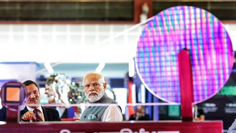
The official announcement was made at ‘Semicon India 2023’ in Gujarat on Friday. This MoU aims to collaborate on the creation of a customised course offering for Indian colleges to teach semiconductor manufacturing technologies using Lam Research’s SemiverseTM Solutions virtual fabrication software called SEMulator3D, which is a 3D semiconductor process and integration modelling platform.
According to Lam, the programme is used by the world’s leading semiconductor businesses, manufacturers and foundries to model whole process flows and forecast downstream consequences of process modifications that would otherwise necessitate fab build-and-test cycles. Students will learn to create process flows and undertake automated virtual experiments that are not possible in the actual fab by using SEMulator3D.
The initiative, which is set to begin in August with a cohort of 30 students, will also concentrate on device integration including physical design learning, process flow development and virtual metrology. The framework pilot course syllabus will be developed by IISc and Lam Research, with the first stage projected to be finished by December 2023 and the second stage by June 2024.
Once the pilot course is successful, IISc and Lam Research want to collaborate with the centre and the Karnataka government to find out the possibility of expanding the relationship with additional universities inside and outside India.
Following the trial with IISc, Lam Research also intends to connect this curriculum to that of the All India Council for Technical Education (AICTE), with the goal of upskilling 60,000 engineers in the next 10 years. Since establishing its first facility in India two decades ago, Lam has expanded its presence in the country’s semiconductor industry; it has most recently opened a state-of-the-art India centre for engineering in Bengaluru dedicated to the development of new technologies required in an era of increasing semiconductor manufacturing complexity.
Since 2014, Lam India has been a member of CeNSE’s industry affiliate programme (IAP) and has worked with the centre on a variety of creative initiatives to enhance the state of semiconductor technology.
“IISc has been a longstanding partner for Lam Research in India and we are happy to extend our relationship to help spur talent development in the semiconductor industry. We anticipate that our relationship with IISc will play an instrumental role in helping to upskill engineers and address workforce requirements as India evolves as a semiconductor manufacturing hub,” said Rangesh Raghavan, corporate vice-president and GM, at Lam Research India.
“India’s commitment to delivering 85,000 engineers by 2030 requires a transformative approach towards how we educate and train semiconductor engineers. The resources required to build a 2nm fab within a university are cost prohibitive. Training engineers in nanofabrication technologies in a virtual environment using industry-leading tools is a welcome step that will help address India’s semiconductor talent requirements in future,” said Prof Srinivasan Raghavan, chairperson of CeNSE, IISc.
David Fried, corporate vice-president of Semiverse Solutions at Lam Research believes that this course will bring a paradigm shift in the education and training of the future Indian semiconductor workforce at greater speed and significantly reduced cost.


Comments
0 comment